You are here
Components and devices
Circuits technology
Presentation :
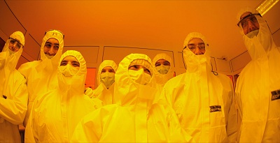
XLIM Circuits Technology Center gathers clean room ressources for Micro and Nano Technologies development as RF MEMS, MOEMS, polymer materials for electro-optic applications and innovative oxyde materials. It is one of the main technological equipment for laboratory research projects and includes researchers, teachers researchers, engineers, technicians and PhD students. Applications are in microwaves, optics and biology.
Technological Facility and Equipments
Processing for MEMS, NEMS and 3D micromachining
I/ Technological Facility and Equipments.
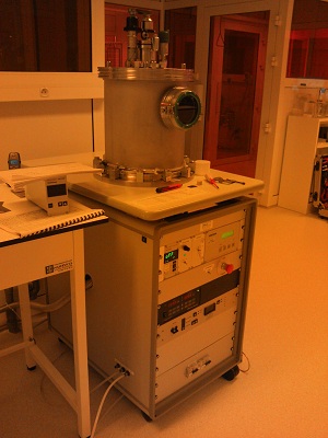
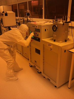
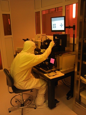
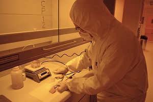
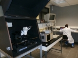
The clean room processing is conducted in a 180 m ² clean room (divided in two classified ISO areas). It includes equipments for microelectronic modeling and manufacturing with emphasis on ceramics and oxides substrates .
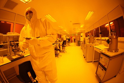
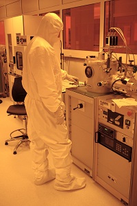
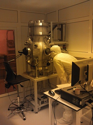
Deposition and Back-end Area
Equipments are used for thin film deposition(from a few nanometers to a few micrometers thicknesses). Several techniques are available (evaporation, assisted sputtering or pulsed laser deposition) at low and very low pressure to obtain high quality films. Micro an Nano Technology Center includes these equipments :
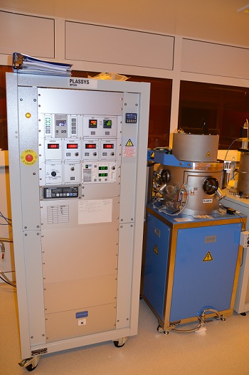
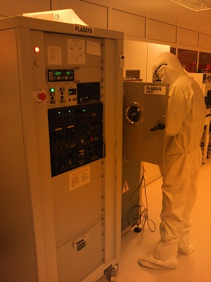
- Two DC cathodic sputtering vacuum chambers (PLASSYS MP300) dedicated to metal deposition (Mo, Al, Ti, Cu) and nitrured materials (AlN), which one have a RF cathode dedicated to dielectric materials (ZnSiO2...),
2" DC and 3" RF cathodic sputtering vaccum chamber (PLASSYS MP300)
3" DC cathodic sputtering vaccum chamber (PLASSYS MP300)
- A thermal evaporator vacuum chamber (Meca 2000) dedicated to metal deposition (Cr, Au, Ti, Al, SiCr, Cu),
Thermal evaporator vacuum chamber (Meca 2000)
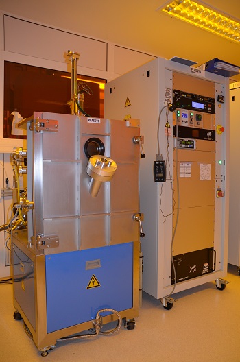
- A thermal evaporator/DC cathodic sputtering (PLASSYS MEPS 300) dedicated to metal films (Cr, Ti, Au/Pd),
Thermal evaporator/DC cathodic sputtering (PLASSYS MEPS 300)
- A vacuum chamber (Meca 2000) with pulsed excimer KrF laser (Compex Pro 110 Lambda Physik) for thin films materials development (Al, Ag, Al2O3, C, Ni, Ru), associating multi-layered film and doping. This process has been developed gathering expertise and know-how between XLIM laboratory and SPCTS laboratory.(http://www.unilim.fr/spcts)
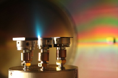
A vacuum chamber (Meca 2000) (PLD : Pulsed Laser Deposition)
- Two E-Beam evaporators (PLASSYS MEB 300 and MEB 400) for metal thin film deposition (Cr, Au, Ti, Al, Cu, Pt, Ni),
E-Beam evaporator (PLASSYS MEB 300)
E-Beam evaporator (PLASSYS MEB 400)
- E-Beam deposition PLASSYS MEB 500 for vanadium dioxyde (VO2). 3 independent beams can be used for composite material deposition.
E-Beam deposition (PLASSYS MEB 500)
- A RIE plasma etching (PLASSYS MG 200) with O2, Ar, N2, SF6, CHF3 reactive gases for metallics and nitride materials etching,
RIE plasma etching (PLASSYS MG 200)
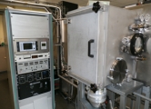
- A plasma PECVD process chamber for dieclectric materials deposition (SiN, Si3N4...),
PECVD equipement
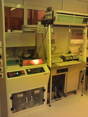
Other back end equipements are available such as :
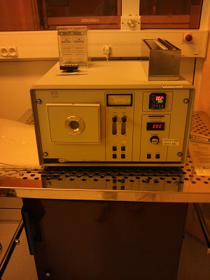
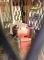
- Two 900°C annealing ovens vaccum or gases controlled,
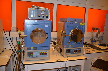
Annealing ovens
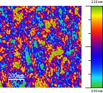
- A 2,5 µm and 12,5 µm stylus profiler Dektak-XT for 3D stress measurement, Atomic Force Microscopy and tribology measurement,
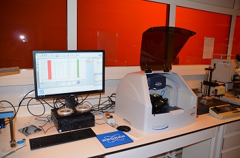
Dektak-XT stylus profiler
- NéoScope JEOL SEM for component observation,
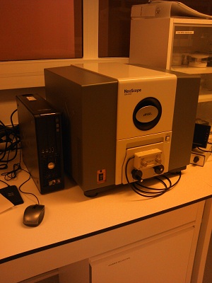
Scanning Electron Microscopy
- DAD3220 DISCO semi automatic dicing saw up to 6 inches wafers,
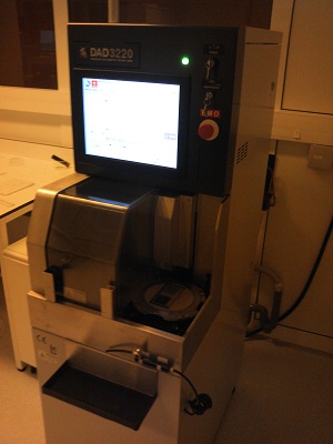
Semi automatic dicing DAD3220 DISCO
- CO2 critical point drying system for MEMS and NEMS
- A Pick and Place machine for surface mounting of components,
- A KS4526 wire bonding machine.
60 m² ISO5 clean room
The equipments in this room are being used for photolithigrapy and surface/bulk micromaching of RF and optic components:
- Two mask aligners KARL SUSS MJB3 et MJB4 up to 4 inches,
Mask aligners KARL SUSS MJB4
- Three spiners Karl SUSS RC8 / Spin Coater 150 for polymers and photoresits,
Spiners
- An O2 plasma etcher,
O2 plasma etcher
- Three ASEM Fume Cabinets EN 14175 for photoresist processing, wet etching, and solvents(Acétone, IPA, ethanol, NMP),
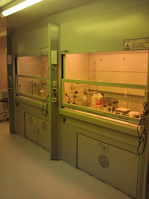
ASEM Fume Cabinets EN 14175
- An electroplating bench (Au, Au/Ni) and electroless copper 3D plating,
Electroplating bench
II/ Processing for MEMS, NEMS and 3D micromachining
Processes have been developped for surface micromachining, bulk silicon etching and 3D ceramic processing.
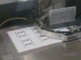
Most components are being done using photolithography, down to sub micrometer scale. Conventionnal photoresist processing (S1805, S1813, S1828, SU8, AZ5214, AZ15nxT) and polymers (PMGI SF6, PMGI SF9, PMGI SF11) permit to obtain 5µm patterns. Some examples are show below:
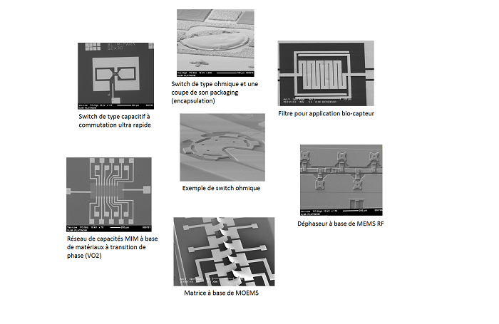
All laboratory research groups are using the clean room for fabrication. Electro-optics plastic team use micro-electronics technologies available within PLATINOM for specific applications.
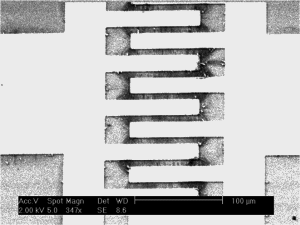
Composant planaire à électrodes interdigitées
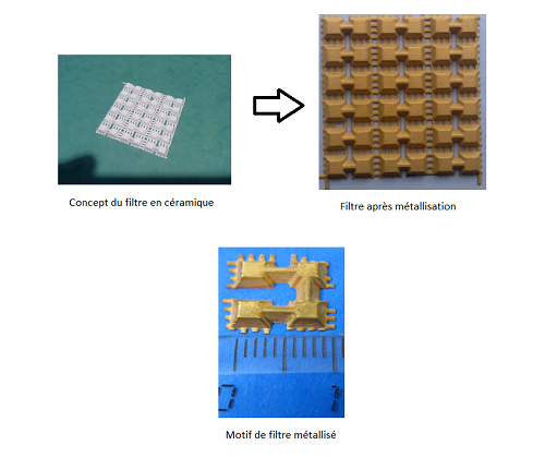
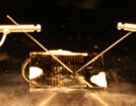
3D ceramic components are being processed in the clean room for 3D metal covering and photolithography. Examples fabricated in cooperation with CTTC are shown below:(http://www.cttc.fr)
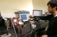
Printed Electronic Technologies and Instrumentation
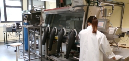
The "Printed Electronic Technologies and Instrumentation" at XLIM brings together a set of fabrication and characterization techniques dedicated to the development of organic/hybrid optoelectronic and printed electronic devices (photovoltaic cells, field-effect transistors, light-emitting diodes, sensors, etc). A specific instrumentation (glove boxes under inert atmosphere) allows the implementation of various components based on organic semiconductors, such as pi-conjugated polymers and small molecules. Both wet and dry processing technologies, as well as available printing technologies (screen-printing and inkjet printing), are compatible with a large choice of configurations and architectures. The physical characterization (morphology, optical and electrical properties) of the devices aims at giving a better understanding of the involved physical and photo-physical mechanisms and the optimization of the architectures and of their functionalities.
The platform is developped and maintained by the ELITE team members, who manage on a day to day basis the set of equipment available.
- Responsibles: bernard.ratier@unilim.fr / johann.boucle@unilim.fr
- Contacts / enquiries for internal and external prestations: permanents.elite@xlim.fr
Fabrication technologies
Dry processing technologies (physical methods)
- Thermal evaporation under vacuum : organic materials / metallic electrodes / interfacial layers (3 benches)
- Electron gun evaporation bench (metallic contacts) under inert atmosphere
- Ion beam sputtering (2 benches) : electrodes, transparent conductive oxides, inorganic materials
- Ion beam assisted deposition (IBAD)
Wet processing technologies (from solution)
- Ink and composite formulation, dispersion of nano-objects (ultrasonic probe)
- Contact angle / Surface tension / viscosity measurements
- Deposition by spin-coating (3 equipments)
- Deposition by screen-printing
- Inkjet printer Fujifilm Dimatix DMP-2831
Specific equipements
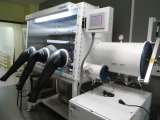
- Glovebox under inert atmosphere including wet and dry processing technologies (spin-coater and thermal evaporation benches).
- Glovebox under inert atmosphere for optoelectronic device characterization (photovoltaic performance, external quantum efficiency, current-voltage characteristics, etc).
- Glovebox under inert atmosphere dedicated to hybrid perovskite materials (spin-coater)
Technologies for the characterization of materials and devices
Morphology
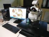
- Optical microscope LEICA DM12000 M
- Mechanical profilometer DEKTAK XT
- Atomic force microscopy AFM, conductive C-AFM, HD-KPFM (ambiant conditions)
Optical characterizations
- UV-visible spectrometer (transmission) SAFAS (300-900 nm)
- Reflectometer AGILENT Cary 300 (reflectometry, optical transmission) : 180 nm - 1010 nm, integrating sphere, for solutions and thin films
- Fluorimeter - Edinburg Instrument FLS980 for steady-state (250-850nm) and lifetime PL measurements (50ps-1s) : integrating sphere, holders for solutions/films/powders
Electrical characterizations
- 4-probe conductivity measurements
- Thermoelectric properties : Conductivity and Seebeck coefficient (77K - 400K, controlled atmosphere)
- Probing station - low frequencies (isolated)
- Dielectric Impedance spectroscopy (up to 120 MHz)
- Semiconductor characterization system Keithley 4200, Source-measure units (various Keithley 24XX and 26XX- up to 5A)
Optoelectronic characterizations
- Two AM1.5G solar simulators (Solarconstant PV275, ORIEL classe A) : under air or under inert atmosphere
- Two certified monocristalline silicon calibration cells
- Experimental set-up for electroluminescence (current-voltage, current-luminance, electroluminescence spectrum)
- Measurement of emission pattern in real space, spectral distribution using a fibered calibrated integrated spectrometer (StellarNet Black Comet)
- External quantum effiicency (EQE or IPCE) : under controlled atmosphere, under static or dynamic regime (lock-in)
- Transient photo-voltage and photo-current measurements (charge kinetics)
- Characterization of PV cells and modules by LBIC / LBIV mapping
![]()


![]()
 UMR CNRS n°7252
123, avenue Albert Thomas - 87060 LIMOGES CEDEX.
Tél. +33(0) 587 50 67 00 - Fax +33(0) 555 45 76 97