- FR
- EN
You are here
OPTOPLAST
Plastic Optoelectronics Technology and Instrumentation (OPTOPLAST)
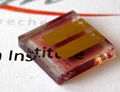
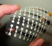

Objectives : The PLATINOM/OPTOPLAST technological facility at XLIM brings together a set of fabrication and characterization techniques dedicated to optoelectronic devices (photovoltaic cells, field-effect transistors, light-emitting diodes, sensors, etc). A specific instrumentation (glove boxes under inert atmosphere) allows the implementation of various components based on organic semiconductors, such as pi-conjugated polymers and small molecules. Both wet and dry processing technologies are compatible with a large choice of configurations and architectures. The physical characterization (morphology, optical and electrical properties) of the obtained devices aims at giving a better understanding of the involved mechanisms and the optimization of the architectures and of their functionalities.
- Contact / external inquiries : optoplast@xlim.fr
- Intranet (internal inquiries, booking of equipments, etc)
2016 Training course "Organic and Hybrid photovoltaic cells" - Cnrs Formation Entreprises / Réseau Nanorgasol
Session open for technicians, Ingeeniers, Researchers. Over 03-October to 05-October 2016. Download the training course flyer.
Dry processing technologies (physical methods)
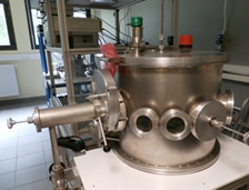
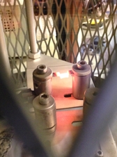
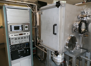
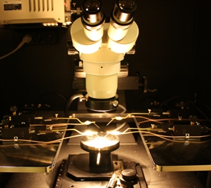
- Thermal evaporation under vacuum : organic materials / metallic electrodes / interfacial layers (3 benches).
- Co-evaporation of organic molecules (1 set-up under inert atmosphere)
- Electron gun evaporation bench (metallic contacts) under inert atmosphere
- Ion beam sputtering (2 benches) : electrodes, transparent conductive oxides, inorganic materials
- Ion beam assisted deposition (IBAD)
Technologies from solution
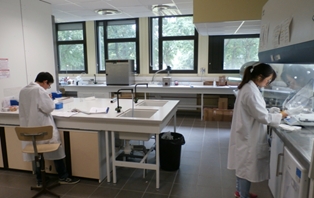
- Ink and composite formulation, dispersion of nano-objects (ultrasonic probe)
- Deposition by spin-coating (2 equipments under air, 1 under inert atmopshere)
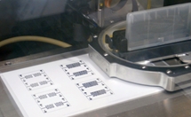
- Deposition by screen-printing
- Ink-jet printer DIMATIX DMP-2831 (Fujifilm)
Specific Equipments
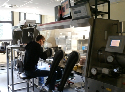
- Glove box under inert atmosphere including wet and dry processing technologies (spin-coater and thermal evaporation benches).
- Glove box under inert atmosphere for optoelectronic device characterization (photovoltaic performance, external quantum efficiency, current-voltage characteristics, etc).
Materials and Devices Characterizations
Morphology
- Mechanical profilometer DEKTAK XT
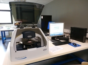
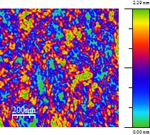
- Atomic Force Microscope CSI Nano Observer: AFM, C-AFM, and KPFM (double lock-in High resolution)
Optical properties
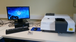
- UV-visible spectrometer (transmission) SAFA (300-900 nm)
- Reflectometer AGILENT Cary 300 (reflectometry, optical transmission) : 180 nm - 1010 nm, integrating sphere, for solutions and thin films
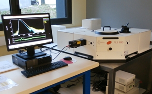
- Spectrophotometer Edinburgh Instrument FLS980 - Steady-state and Transient PL measurements (50 ps to 1 s)
Electrical Characterizations
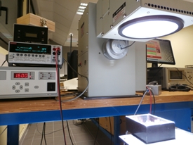
- 4-probe conductivity measurements
- Thermoelectric properties : Conductivity and Seebeck coefficient (77K - 400K, controlled atmosphere)
- Probing station - low frequencies (isolated)
- Dielectric Impedance spectroscopy (up to 120 MHz)
- Semiconductor characterization system Keithley 4200, Source-measure units (various Keithley 24XX - up to 5A)
Optoelectronic Characterizations
- Two AM1.5G solar simulators (Solarconstant PV275, ORIEL classe A) : under air or under inert atmosphere
- Two certified calibration cells
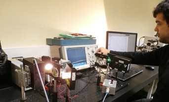
- Experimental set-up for electroluminescence (current-voltage, current-luminance, luminance spectrum)
- External quantum effiicency (EQE or IPCE) : under controlled atmosphere, under static or dynamic regime (lock-in)
- Transient photo-voltage and photo-current measurements (charge kinetics)
- LBIC / LPIV mapping of photovoltaic cells and modules
![]()


![]()
 UMR CNRS n°7252
123, avenue Albert Thomas - 87060 LIMOGES CEDEX.
Tél. +33(0) 587 50 67 00 - Fax +33(0) 555 45 76 97