You are here
MIcro and Nanostructures for Telecommunications - MINT
The MINT team develops RF and high-frequency devices based on functional materials integration or on specific micro-technological processes. The team has a recognized know-how in designing and realising relevant RF/ mW demonstrators using new materials or micro-nano structures.
Research themes developped within MINT
|
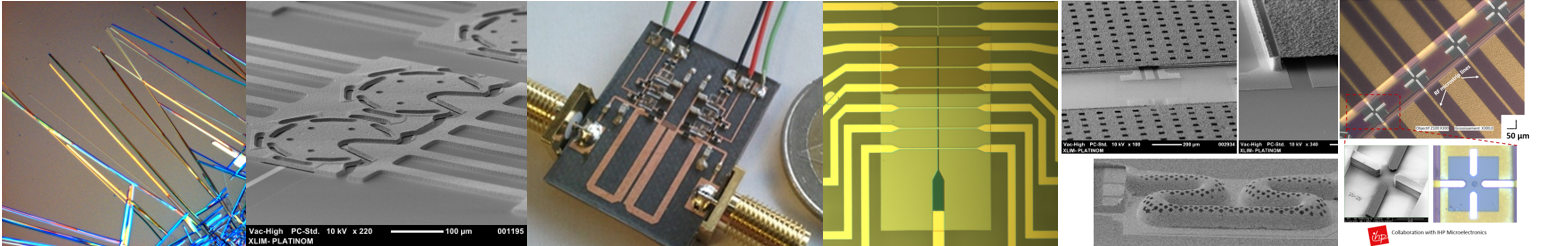
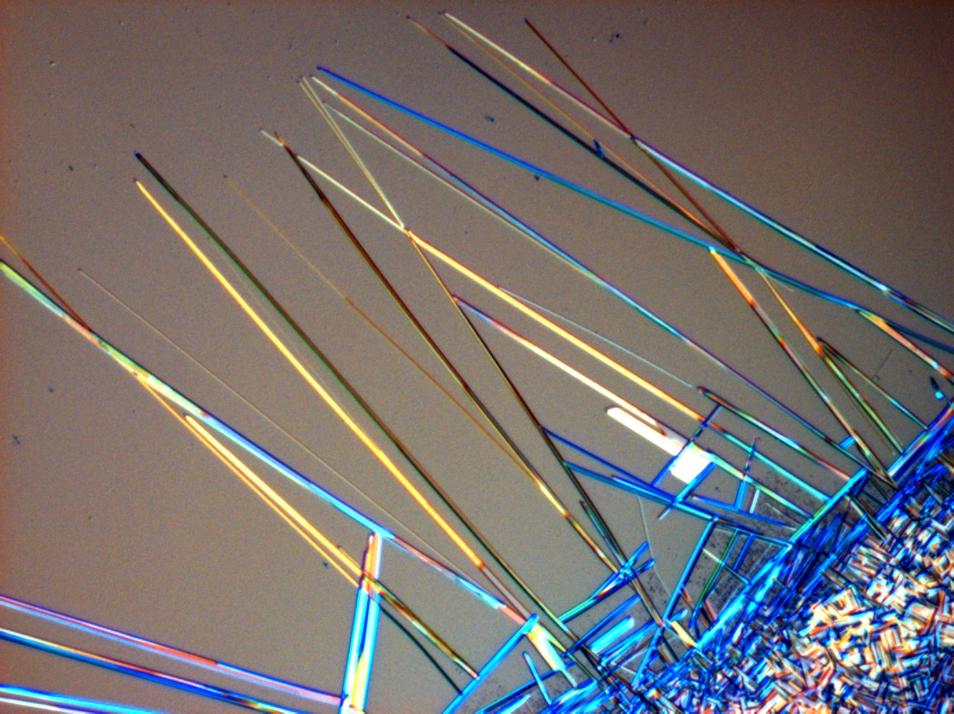
Smart/ Functional MaterialsIntegration of phase transition and phase-change materials (VO2, GeTe, GST ...), ferroelectrics (BST, NBT-BT), piezoelectric materials (ZnO, AlN ...) for advanced high-frequency functions (switches, variable capacitors, acoustic micro-resonators) […] |
RF-MEMS / NEMS devicesSeveral state-of-the-art demonstrators were built– Successful Space-borne launch of RF-MEMS in geostationary orbit (Athena-Fidus satellite Feb 2014). Launching of AirMEMS start-up, 2013 […] |
|
High-Resolution Micro Additive FabricationInnovative additive manufacturing processes are developed for the realization of complex 3D millimeter-wave structures. Fabrication of multi-layer components like air-filled rectangular micro coaxial lines […] |
Tunable microwaves and milimeter waves devicesDevelopment of frequency- reconfigurable or programmable devices (filters, antennas, power amplifiers) – The objective is to explore the potential of the various technologies developed within the team (Smart materials, MEMS, …) relying on our RF modeling abilities to realize next-generation RF and millimeter components […] |
|
|
Micro/ Nanoscale RF SensorsDevelopment of new sensors integrated with CMOS technology. These advanced processes allowed the development of novel systems for characterization of materials (including biological ones) at the nanometer scale […] |
Smart/ Functional Materials
|
|
Integration of phase transition and phase-change materials (VO2, GeTe, GST ...), ferroelectrics (BST, NBT-BT), piezoelectric materials (ZnO, AlN ...) for advanced high-frequency functions (switches, variable capacitors, acoustic micro-resonators). |
-
Intégration des matériaux à transition et à chagement de phase (PTM/ PCM)
These research is oriented toward the development of high-speed switches and high-frequency circuits (microwave, millimeter, THz, optical domains) using phase transition materials (PTM-vanadium dioxide, VO2) or phase change materials (PCM-GeTe, GST) with remarkable properties (significant change in their electrical and optical properties) due to external stimuli (thermal, mechanical, electrical, optical).
- High-frequency applications of PTM materials (VO2)

- Electronics/ optics applications of phase transition materials (VO2)

- Bistable, broadband RF switches based on phase change materials (GeTe/ GST)
We target the development of emerging devices incorporating phase change materials (GeTe / GST) for the realization of the bistable hyper frequency agile functions (switches, filters, antennas ...) in the microwave, millimeter wave, THz domains using electrical and optical excitations.

-
Tunable capacitors based on ferroelectric materials (BST)
ECollaboration with n collaboration avec le laboratoire SPCTS laboratory, XLIM's Antennas & Signals team and NIMP Institute (Romania)- ANR project-Maestro and H2020 project M-EraNet MASTERS (EU)

We exploit the agility of BST (Ba1-xSrxTiO3) ferroelectric materials (change of their permittivity under an external electric field) to develop electrically tunable capacitors using MFM (Metal-Ferroelectric-Metal) or IDT topologies (inter-digit electrodes). The main objective of this research action is to introduce new components / devices with suitable properties for the realization of reconfigurable antennas in the ISM frequency band (Industrial, Scientific and Medical) (around 2.45 GHz) and at millimeter waves ( 30 GHz to 64 GHz).
-
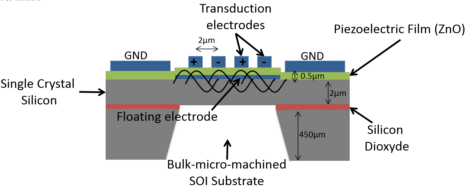
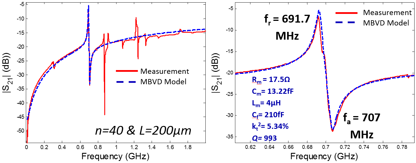
Acoustic micro-resonators integrating piezolectric materials (ZnO, AlN)
This research theme focus on the design and realization of suspended piezoelectric micro-resonators integrating thin layers of ZnO and AlN with state of the art performances (coupling coefficients, quality factors).
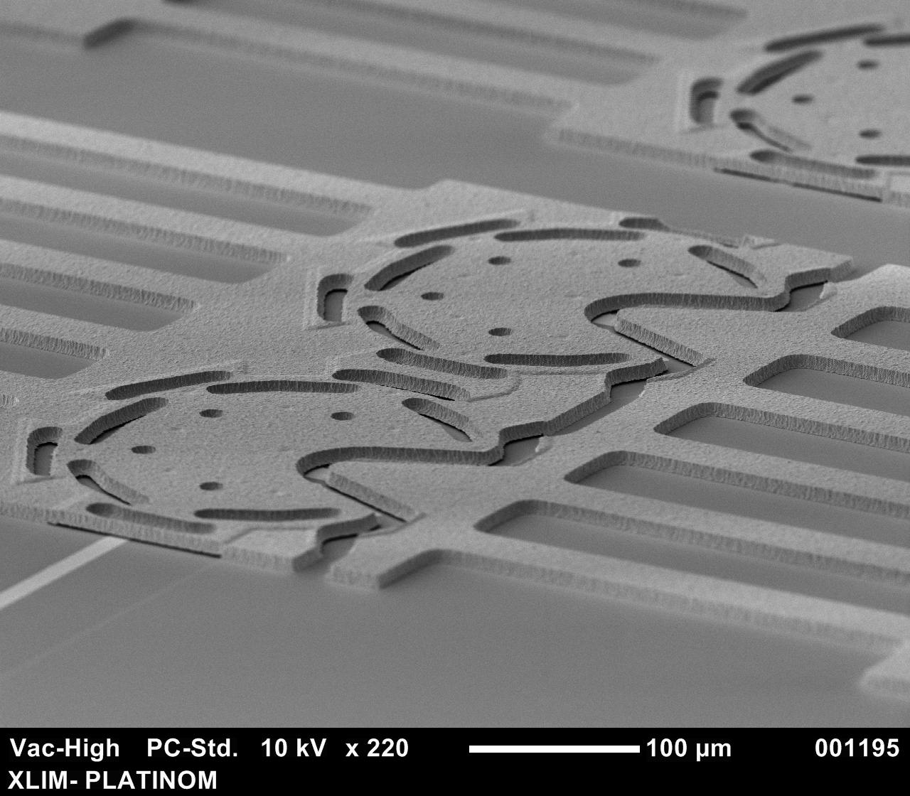
RF- MEMS/ NEMS devices
|
|
Several state-of-the-art demonstrators were built. Successful Space-borne launch of RF-MEMS in geostationary orbit (Athena-Fidus satellite Feb 2014). Launching of AirMEMS start-up, 2013. |
-
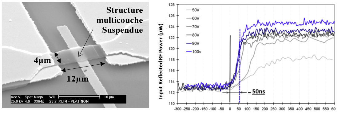
Development of mechanical architecture for RF MEMS components for achieving a fast reconfiguration – CNRS highlight - 2011
To reduce the switching speed, miniature MEMS have been designed and fabricated. For MEMS switches, the electrical switching speed is generally limited to a few microseconds, inherently restricted by the delay required to mechanically move their mobile membrane up and down. Miniature bridges have been built by using a proper mechanical design and the structural material fabrication process with mechanical resonance frequencies over 10 MHz. As a result, the switching speed of these miniature components is greatly improved and reaches 50 to 100 ns. Such performance has been achieved using composite micro-beams based on the multilayer material assembly of alumina/aluminum/alumina.
-
Development of an air gap MEMS with one mechanical stop to increase its lifetime and reliability
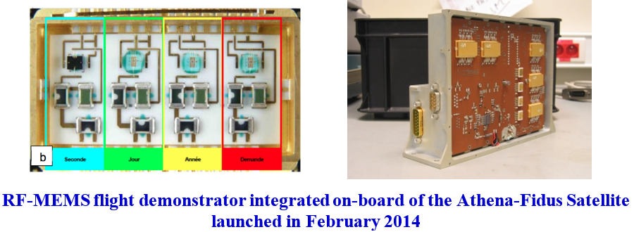
One of the highlight of the team is the development of an air gap MEMS with a mechanical stop to increase its lifetime and reliability. These RF microswitches have been integrated into the payload of the Athena-fidus satellite launched in February 2014. This world first made it possible to validate the MEMS technology of the laboratory and also aims at obtaining a spatial qualification. This project was financed by the French National Center for Space Studies (CNES) and led by Thales Alenia Space.
|
|
This work also led to the creation of the Airmems start-up in 2013. AirMems is able to provide customized efficient RF circuits (filters, phase shifters, impedance matching networks, single ports-N-throws…) using RF-MEMS switches, over a wide frequency band. |

-
Development of MEMS-RF with figure of merit less than 10 fsec
|
|
Recently elaborate components achieve figure of merit (Ron x Coff) of less than 10 fsec using a thin film package. Developed with the support of the DGA, this technology is the subject of patent application. |
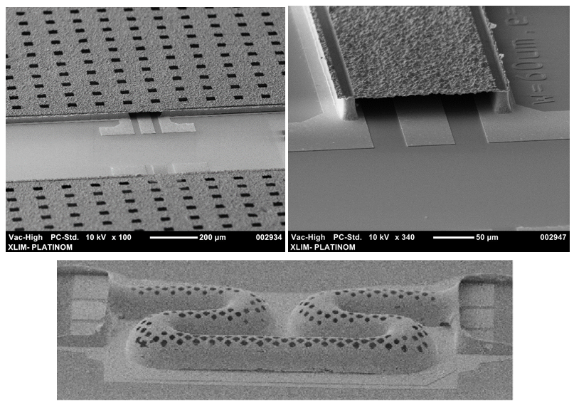
High-Resolution Micro Additive Fabrication
|
|
Innovative additive manufacturing processes are developed for the realization of complex 3D millimeter-wave structures. Fabrication of multi-layer components like air-filled rectangular micro coaxial lines. |
Tunable microwaves and millimeter wave devices
|
|
Development of frequency- reconfigurable or programmable devices (filters, antennas, power amplifiers) – The objective is to explore the potential of the various technologies developed within the team (Smart materials, MEMS, …) relying on our RF modeling abilities to realize next-generation RF and millimeter components. |
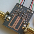
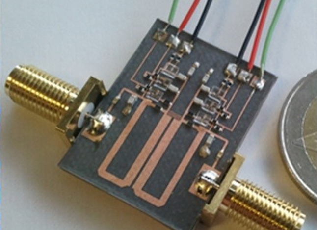
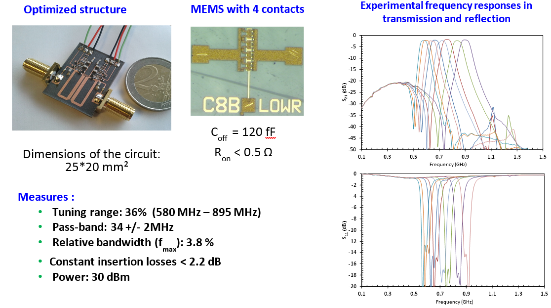
Examples of Tunable Filters and Agile Antennas integrating MEMS devices
-
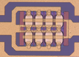
A two-pole tunable bandpass filter using RF-MEMS switches
New approaches have been developed to design tunable band-pass filters with constant bandwidth and wide tuning range for the 520 - 860 MHz wireless band. The filter consists of two-coupled hairpin resonators loaded by a tuning capacitor. MEMS switches with four ohmic contacts are used.
-
A 3-bit Frequency Tunable PIFA Antenna using MEMS technology
Collaboration with Antennas&Signals team
A compact Planar Inverted F-Antenna has been designed, fabricated and characterized. The antenna center frequency can be tuned from 1.52 GHz up to 2.25 GHz, using switched auxiliary strips. Ohmic contact RF-MEMS switches are used to connect and disconnect the auxiliary strips, maintaining both efficiency and antenna linearity. The efficiency of the PIFA antenna measured for all states in an anechoic chamber, ranges from 52% up to 95%. The antenna linearity has also been measured using an Adjacent Channel Power Ratio (ACPR) test bench, showing 42 dB dynamic range up to 28 dBm input power.

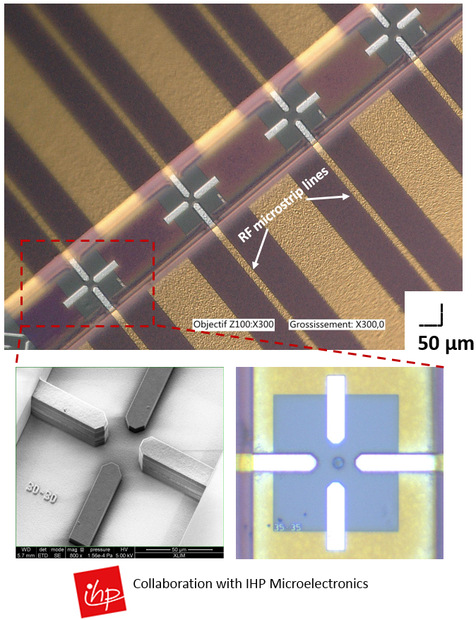
Micro/ Nanoscale RF Sensors
|
|
Microfluidic microsystems implemented on Bipolar-Complementary Oxide Semiconductor (BiCMOS) technology for single cells handling. UHF frequencies (above 100 MHz) dielectrophoresis technique for intracellular dielectric properties cell discrimination. |

SUMCASTEC - Semiconductor-based Ultrawideband Micromanipulation of CAncer STEm Cells
Project ID : 737164// : H2020-EU.1.2.1. - FET Open // From 2017-01-01 to 2020-06-30
SUMCASTEC explores a radically new approach for isolating and neutralizing cancer stem cells through semiconductor-based ultrawideband micromanipulation. Coordinator: Université de Limoges, France.
SUMCASTEC explores radically new approach for cancer stem cells (CSCs) real time isolation (i.e. within minutes vs current 40 days) and neutralization. A novel micro-optofluidic lab-on-chip (LOC) platform will be developed through a joint and iterative effort by biologists, clinicians and engineers. For the first time, a single LOC will be capable of delivering ultra-wide broadband radiation to compare cell spectral signatures, image subcellular features, and hence modulate CSCs microenvironment conditions with unprecedented space and time resolution. It will be driven to isolate CSCs from heterogeneous differentiated and stem cell populations, and force CSCs differentiation, ultimately inducing sensitivity to anticancer treatments. Extensive in vitro and in vivo testing along with biophysical modelling will validate the approach and establish the proof-of-principle within the project life-time, while laying the groundwork for further development of future electrosurgical tools that will be capable CSCs neutralization in tissue.
This will not only establish a new line of treatment for brain cancers such as Glioblastoma Multiforme and Medulloblastoma, whose initiation and recurrence were linked to CSCs, and that claim tremendous human and economic tolls, worldwide; it will also push the current boundaries of microbiological analysis by enabling microenvironment characterization/manipulation and real-time ionic channels monitoring without cytotoxic patch-clamping or electron microscopy.
By investing in efforts such as SUMCASTEC’s, Europe will stand at the forefront of global biomedical innovation and push through a similar miniaturization trend as the one that propelled mobile communications, yet with much deeper societal impact.
Participants
BANGOR UNIVERSITY (United Kingdom)
IHP GMBH - INNOVATIONS FOR HIGH PERFORMANCE MICROELECTRONICS/LEIBNIZ-INSTITUT FUER INNOVATIVE MIKROELEKTRONIK (Germany)
AGENZIA NAZIONALE PER LE NUOVE TECNOLOGIE, L'ENERGIA E LO SVILUPPO ECONOMICO SOSTENIBILE (Italy)
UNIVERSITA DEGLI STUDI DI PADOVA (Italy)
CREO MEDICAL LIMITED (United Kingdom)
![]()


![]()
 UMR CNRS n°7252
123, avenue Albert Thomas - 87060 LIMOGES CEDEX.
Tél. +33(0) 587 50 67 00 - Fax +33(0) 555 45 76 97