- FR
- EN
You are here
Circuits Technology Center
Presentation :
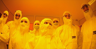
XLIM Circuits Technology Center gathers clean room ressources for Micro and Nano Technologies development as RF MEMS, MOEMS, polymer materials for electro-optic applications and innovative oxyde materials. It is one of the main technological equipment for laboratory research projects and includes researchers, teachers researchers, engineers, technicians and PhD students. Applications are in microwaves, optics and biology.
Technological Facility and Equipments
Processing for MEMS, NEMS and 3D micromachining
I/ Technological Facility and Equipments.
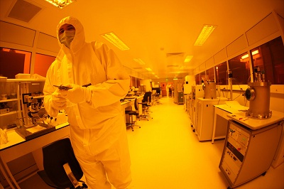
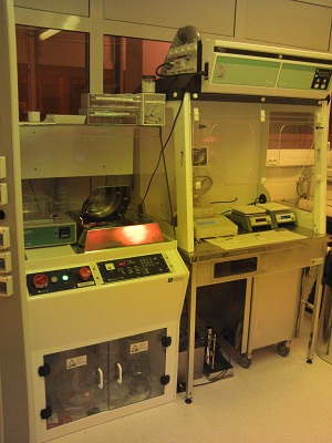
The clean room processing is conducted in a 180 m ² clean room (divided in two classified ISO areas). It includes equipments for microelectronic modeling and manufacturing with emphasis on ceramics and oxides substrates .
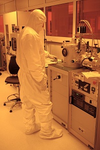
Deposition and Back-end Area
Equipments are used for thin film deposition(from a few nanometers to a few micrometers thicknesses). Several techniques are available (evaporation, assisted sputtering or pulsed laser deposition) at low and very low pressure to obtain high quality films. Micro an Nano Technology Center includes these equipments :
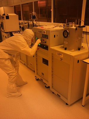
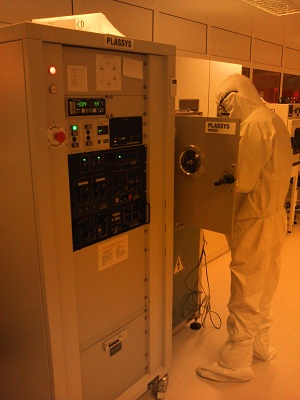
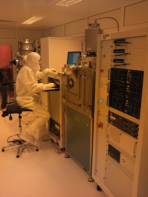
- A DC cathodic sputtering vacuum chamber (PLASSYS MP300) dedicated to metal deposition (Mo, Al, Ti, Cu) and nitrured materials (AlN),
DC cathodic sputtering vacuum chamber (PLASSYS MP300)
- A thermal evaporator vacuum chamber (Meca 2000) dedicated to metal deposition (Cr, Au, Ti, Al, SiCr, Cu),
Thermal evaporator vacuum chamber (Meca 2000)
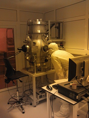
- A thermal evaporator/DC cathodic sputtering (PLASSYS MEPS 300) dedicated to metal films (Cr, Ti, Au/Pd),
Thermal evaporator/DC cathodic sputtering (PLASSYS MEPS 300)
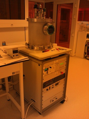
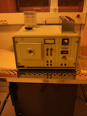
- A vacuum chamber (Meca 2000) with pulsed excimer KrF laser (Compex Pro 110 Lambda Physik) for thin films materials development (Al, Ag, Al2O3, C, Ni, Ru), associating multi-layered film and doping. This process has been developed gathering expertise and know-how between XLIM laboratory and SPCTS laboratory.(http://www.unilim.fr/spcts)
A vacuum chamber (Meca 2000) (PLD : Pulsed Laser Deposition)
- E-Beam evaporator (PLASSYS MEB 300) for metal thin film deposition (Cr, Au, Ti, Al, Cu),
E-Beam evaporator (PLASSYS MEB 300)
- E-Beam deposition PLASSYS MEB 500 for vanadium dioxyde (VO2). 3 independent beams can be used for composite material deposition.
E-Beam deposition (PLASSYS MEB 500)
Other back end equipements are available such as :
- NéoScope JEOL SEM for component observation,
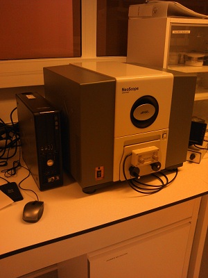
Scanning Electron Microscopy
- DAD3220 DISCO semi automatic dicing saw up to 6 inches wafers,
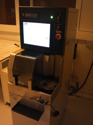
Semi automatic dicing DAD3220 DISCO
- CO2 critical point drying system for MEMS and NEMS
- A Pick and Place machine for surface mounting of components,
- A KS4526 wire bonding machine.
60 m² ISO5 clean room
The equipments in this room are being used for photolithigrapy and surface/bulk micromaching of RF and optic components:
- Two mask aligners KARL SUSS MJB3 et MJB4 up to 4 inches,
Mask aligners KARL SUSS MJB4
- Three spiners Karl SUSS RC8 / Spin Coater 150 for polymers and photoresits,
Spiners
- An O2 plasma etcher,
O2 plasma etcher
- Three ASEM Fume Cabinets EN 14175 for photoresist processing, wet etching, and solvents(Acétone, IPA, ethanol, NMP),
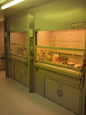
ASEM Fume Cabinets EN 14175
- An electroplating bench (Au, Au/Ni) and electroless copper 3D plating,
Electroplating bench
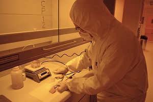
II/ Processing for MEMS, NEMS and 3D micromachining
Processes have been developped for surface micromachining, bulk silicon etching and 3D ceramic processing.
Most components are being done using photolithography, down to sub micrometer scale. Conventionnal photoresist processing (S1805, S1813, S1828, SU8, AZ5214, AZ15nxT) and polymers (PMGI SF6, PMGI SF9, PMGI SF11) permit to obtain 5µm patterns. Some examples are show below:
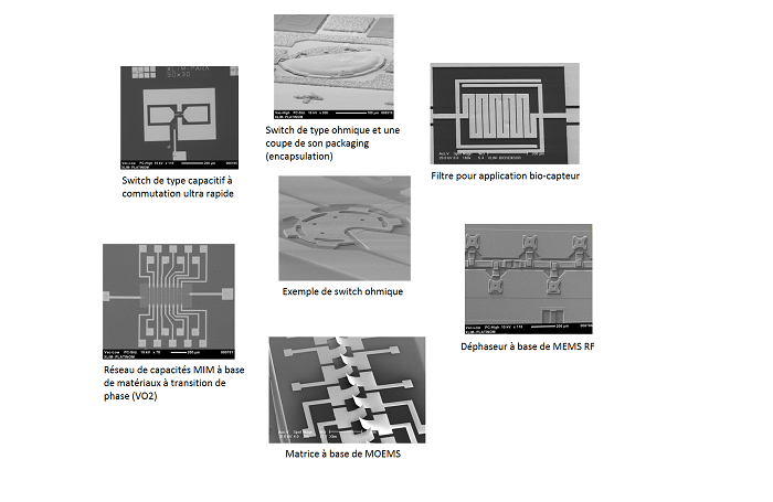
All laboratory research groups are using the clean room for fabrication. Electro-optics plastic team use micro-electronics technologies available within PLATINOM for specific applications.
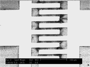
Composant planaire à électrodes interdigitées
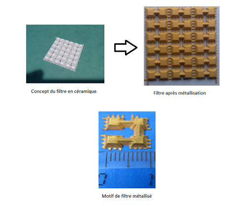
3D ceramic components are being processed in the clean room for 3D metal covering and photolithography. Examples fabricated in cooperation with CTTC are shown below:(http://www.cttc.fr)
![]()


![]()
 UMR CNRS n°7252
123, avenue Albert Thomas - 87060 LIMOGES CEDEX.
Tél. +33(0) 587 50 67 00 - Fax +33(0) 555 45 76 97