MINACOM Department
You are here
MINT - MIcro and Nano structures for Telecom applications
The group MIcro and Nano structures for Telecom applications develops new technologies for micro fabrication of components like:
- RF MEMS-NEMS and MOEMS
- Circuit integration of innovative materials for microwave and optical applications
- Biosensors for cellular characterisation
RF MEMS RF technologies and reconfigurable components
Contact
Pierre BLONDY ( pierre.blondy@xlim.fr )
Involved people
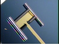
XLIM Dielectric less capacitive RF MEMS switch
Over the past few years, innovative technologies, derived from microelectronics such as surface micromachining have been used for the fabrication of micrometer scale components: RF-MEMS.
This new generation of components has various shapes and functionalities, for many applications. For microwaves and RF, they permit the realization of reconfigurable components with outstanding performances regarding loss or linearity. Our laboratory has developed two internal RF-MEMS fabrication process, for the study of reliability and RF demonstrators.
1.5-2.3 GHz RF MEMS tunable filter on ceramic substrate
We have studied implementation of RF-MEMS in key front end components such as phase shifters, tunable filters and antennas.
13- 23GHz switchable MEMS patch antenna
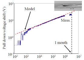
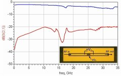
Actuation voltage drift of XLIM RF MEMS switch held in the down state during one month
For reliability issues, our group has developed an automated C(V) test bench for the characterization of charge retention phenomenon?s in electrostatic actuators. Effects of Bias waveforms, environment or temperature can be studied with this bench.
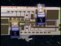
Low temperature and collective non hermetic RF MEMS packaging
At last, several packaging techniques are being studied from O level packaging to 1 level. The effects of packaging on microwave performances and reliability can be studied in our laboratory.
Miniature MEMS RF component based on nanogaps for sub-microsecond switching speed
Contact
Arnaud POTHIER ( arnaud.pothier@xlim.fr )
Involved People

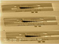
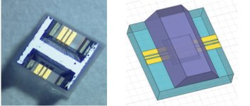
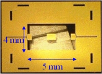
Xlim miniature RF MEMS switch
The main objective of this research activity rely on the design of new RF MEMS switch architecture able to be much faster than conventional MEMS components.MEMS micro-relay switching times are in most of case limited to few microseconds, dominated by the intrinsic mechanical motion speed of their movable part. Using an appropriated design, we have manufactured some miniatures MEMS bridge beams able to mechanically vibrate up to several MHz, against tens of KHz for classical MEMS devices with dimensions 10 to 30 times more large. Such miniature component fastness is hence strongly improved and can be reduced up to hundred of nanoseconds.
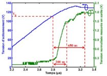
Typical measured minature MEMS switching time
Hence, increasing the MEMS devices mechanical bandwidth up to that one to modulated signal to be transmitted, this new concept of microwave switch can be potentially applied to a wide application domain as MEMS modulators able to work under MBits/s data rate or even else as phase shifter with high speed reconfiguration for smart communication modules (National ANR funded project: SIPCOM 2008).
Network of miniatures MEMS capacitors
This research activity, today move to the fabrication of smaller mechanical switchable devices at the scale of only few microns in the frame of project with Thales Alenia Space company and the CNES (French National Space Agency) as main partners. A part of our current research effort is also focused on the use of new structural material with remarkable mechanical properties as carbon nano-tubes de for example in the frame SIMS a National ANR funded project since 2007 in collaboration with Thales company and the LPCIM lab part of Ecole Polytechnique.
Integration of smart materials with advanced functionalities in microwave and optical devices and systems
Contact
Aurelian CRUNTEANU STANESCU ( aurelian.crunteanu@xlim.fr )
Involved People
- Pierre BLONDY
- Arnaud POTHIER
- Jean Christophe ORLIANGES
- Agnes DESFARGES
- Vincent KERMENE
- Vincent COUDERC
- Corinne CHAMPEAUX (SPCT UMR 6638)
- Alain CATHERINOT (SPCT UMR 6638)
The main objective of this research activity is to develop new types of ultra-fast switches operating in the RF- microwave and optical domains by using a class of materials undergoing fast reversible transitions from a semiconducting state to a metallic one (semiconductor ?metal transition ? SMT). The final goal is to realize commutation functions allowing improving the current problems encountered in the communication systems (consumption, power handling, fast switching and integration).
RF performances of VO2 series switch: OFF state (lower, red curve) and ON state (upper, blue curve)
As an example, the reversible SMT transition of the VO2 thin films can be triggered by different external excitations (temperature, optically or electrically by charge injection) and can be as fast as several hundreds of femtoseconds (fs). During the phase transition the electrical resistivity of the VO2 thin films can decrease by several orders of magnitude while from the optical point of view, the material is transparent in the semiconductor phase and highly reflective in metallic state for a large spectral domain (from 1um up to the THz frequencies). We are exploiting these remarkable properties of the VO2 material for switching or deviating incoming electromagnetic fields propagating in microwave coplanar waveguides integrating a thin VO2 film (on/ off switching during the fast changing of VO2 resistivity during an SMT transition). For the optical commutation applications we are employing the reflectivity change of a VO2 thin films undergoing an SMT transition in order to realize variable reflectivity micro-mirrors (rapid optical commutation) with a large application area (optical modulators for obtaining short laser-pulse in the Q-switching or mode-locking regime, optical switches etc.).

VO2 based optical switch ...

... electrically activated
This research activity is developed in collaboration with the SPCTS laboratory and with the XLIM's Photonics Department. It is partly supported by ANR through the project "Advanced microwave and optical switching devices based on reversible Metal-Insulator Transition (MIT) in VO2 thin films"- ADMOS-VO2 (ANR-07-JCJC-0047, Aurelian Crunteanu).
High frequency filtering using micromachined techniques
Contact
Matthieu CHATRAS ( matthieu.chatras@xlim.fr )
Involved People
Silicon micromachining consist in suspending a circuit on a thin dielectric membrane by removing the substrate. Field propagation will then occur in air, reducing the main problems of planar devices, such as losses. Quality factor over than 600 can then be obtained (state of the art). Filters with relative bandwidth close to 1% can then been developed with low insertion losses.
Micromachined structure: Cross section
Membrane suspended resonator
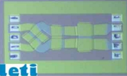
Lots of collaborations have been carried out with Thales Alenia Space and ESA (European Space Agency). Band-pass filters have been achieved from 20 to 150 GHz with very good results.
20GHz 4 pole micro machined filter
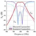
150GHz 2 pole micro machined filter
Bulk Acoustic Wave (BAW) devices
Contact
Matthieu CHATRAS ( matthieu.chatras@xlim.fr )
Involved People
Vibration properties of piezoelectric materials are used to achieve filtering functions. The mainly used material is Aluminum Nitride (AlN), due to its good electrical and acoustical properties. The different devices are achieved in the GHz range (1-5 GHz). Lots of collaborations have been carried out with CEA-LETI, CNES, and DGA (French army). Xlim is involved in different European or French research programs.One of the main difficulties during BAW filter synthesis is to be able to predict in a very efficient way the behavior of the device. Global simulation and optimization methods have then been developed. These methods are based on the description of piezoelectric equations in 1D, 2.5D and 3D. Very good measurement results have enabled to validate our computation tools for BAW devices.
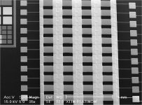
ALN based BAW resonator
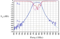
6 pole UMTS BAW filter
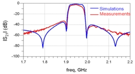
UMTS BAW filter measurements
MOEMS- type micro-mirrors integration in complex optical systems
Contact
Aurelian CRUNTEANU STANESCU ( aurelian.crunteanu@xlim.fr )
Involved People
The association of micro-optics and micro-electro-mechanical systems (MEMS) creates a new and relatively broader area of devices, the micro-opto-electro-mechanical systems (MOEMS). Their properties (compact, scalable, low insertion losses, low cross-talk, polarization insensitive, high speed and batch, low-cost production) along with their emerging functionalities as optical switches, micro-scanners, and variable attenuators/shutters find extensive applications in telecommunications, astrophysics, biology, imaging etc.
Array of bridge-type micro-mirrors
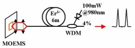
Micro mirrors integration as a Q-switch modulator in a pulse fibre lasers system

Asynchronous and synchronous electrostatic actuation of cantilever-type micro-mirror array
Within this framework, the research activities developed in our Institute (through a close collaboration between the MINACOM and Photonics Departments) are oriented towards the integration of MOEMS elements (bridge- or cantilever-type membranes serving as light modulators or spectral selectors) for fabrication of miniature laser sources with short pulses and variable repetition rates. The main objectives of this research activity are to realise novel optical systems with complex, advanced functionalities (short-pulse, variable frequency dual wavelength fiber lasers, spectral selectivity systems including a supercontinuum light source etc.).
Biosensors dedicated to cellular characterization at microwave frequencies: application to label free lab on chip devices
Contact
Arnaud POTHIER ( arnaud.pothier@xlim.fr )
Involved People
- Fabrice LALOUE (Faculté de Medecine de Limoges) fabrice.lalloue@unilim.fr
- Marie-Odile JAUBERTEAU (Faculté de Medecine de Limoges)
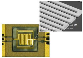
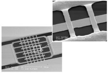
MEMS Biosensors devices manufactured in XLIM Lab
This recent activity is born from a collaboration with a Limoges Faculty of Medecine research group (Homéostasie cellulaire et Pathologie EA 3842) in which the main idea was to propose new generation of biosensors especially designed for the biocellular characterization and identification at microwave frequencies. Hence this work has permitted up to now to develop devices specifically designed at the cell scale thanks to micro-machined technologies. These biosensors are able to discriminate different cellular type without any specific labeling and so avoid the contamination of the biological media and the influence of the marker on the cell properties.
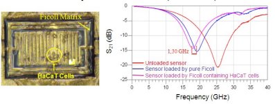
Influence of tens of human tumorous cells on the biosensors performance
The developed biosensor enhance sensitivity allows up to now to work with only tens of biological cells with a good spectral resolution. Hence it is possible to extract with a good accuracy individual analyzed cell electrical properties and so to discriminate them.Today, we are working to establish an intrinsic electromagnetic signature for different cell type using micro-fluidic technologies for their single cell analysis capabilities.
![]()


![]()
 UMR CNRS n°7252
123, avenue Albert Thomas - 87060 LIMOGES CEDEX.
Tél. +33(0) 587 50 67 00 - Fax +33(0) 555 45 76 97