You are here
ELITE
The ELITE team is involved in the fundamental and experimental research on organic and hybrid optoelectronics for telecom and energy applications, from the integration of materials, fabrication of devices, their optoelectronic characterization, to the numerical modeling of their physcial properties. The ELITE team focus on the development of a large variety of devices.
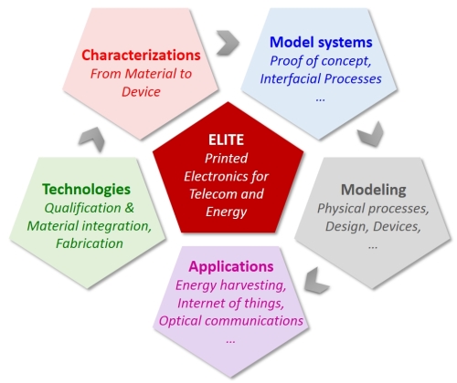
The specific know-how of the team relates to the integration of new materials, the physics of thin films and interfaces, the development of new device architectures, their electrical and optical modeling, extended to printed electronics, and expoits the PLATINOM technological plateform at XLIM, which combines a wide range of fabrication (physcial deposition method and processes from solution) and characterization (optical and electrical properties, morphology, optoelectronic properties) technologies. One of the main objectives is to address four of the six Key enabling Technologies of the European Union strategy (Nanotechnology, Advanced Materials, Photonics, and Advanced fabrication processes).
The group was (and still is) principal coordinator of several granted research projects, and developped several collaboration with local and non local industrial partners for the development of printing technologies devoted to organic solar cells (for example).
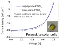
New : Video of a 0.2cm² active area perovskite solar cell
Contact : permanents.elite@xlim.fr
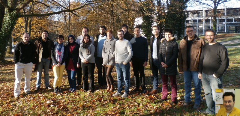
The ELITE Team (2015)
Core activities
Technologies of fabrication
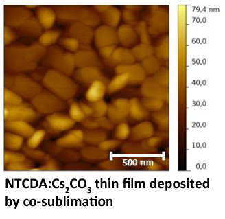
Since more than two decades, the ELITE team focuses on the processing and integration of organic and inorganic semiconducting materials in optoelectronic devices, using physical deposition methods (sublimation, co-sublimation), as well as processes from solution. Ion-beam assisted technologies (IBS, IBAD) also remain an historical skill of the group.
Towards printed electronics
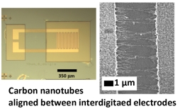
Since the last ten years, the group specializes in processes from solution which can be compatible with low cost and large area, such as screen-printing or inkjet printing technologies. The team takes benefit from a specific expertise regarding ink formulation and rheology (organic blends, composites, dispersion of nano-objects, etc).
The main technologies exploited in the group define the "Printed electronic" domain of the PLATINOM / Devices and Circuits platform, which constitutes a national technlogical platform for printed electronics.
Electrical properties
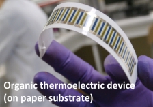
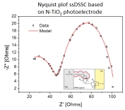
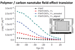
The characterization of the electrical properties of materials and devices is an important step of the group activities. The electrical resistivity are for example measured using the 4-probe method applied on interfacial layers and to transparent electrodes. These two main elements, which are found in most optoelectronic devices, are largely investigated in the group. Moreover, the intrinsic properties of materials can be revealed through their thermoelectric behaviours (measurement of Seebeck coefficient), which can be monitored as a function of temperature. Furthermore, the electrical characteristics of field-effect transistors allow us to extract important parameters of semiconducting materials, such as charge carrier mobilities. The frequency response of samples, probed by impedance spectroscopy, can be used to measure their dielectric permittivity and to identify the transport mechanisms occuring at the different interfaces involved. This wide range of techniques allows us to precisely analyze the electronic processes involved as a function of active layer and device architecture (charge recombination, charge transferts, etc).
Optoelectronic properties
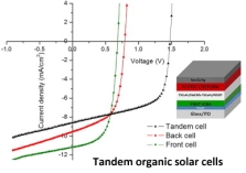
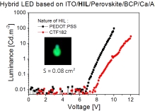
The group is particularly interested by the optoelectronic properties of materials and devices: optical absorption/transmission/reflexion, photoluminescence studies, and performance of final devices. These investigations especially focus on organic systems based on conjugated polymers or small molecules, as well as on hybrid systems combining both organic and inorganic semiconducting materials, or involving perovskite materials (both hybrid and oxyde perovskites). In this context, the physics of interfaces is a major issue addressed by the team, which focuses on interface engineering and advanced characterization of model devices, in order to get a better understanding of the physical processes involved, including light emission, photo-generation, and charge transfert mechanisms. Currently, the targeted applications relate to photovoltaic energy conversion, electroluminscence for visible light communications, energy harvesters, and photodetectors.
New : Video of a 0.2 cm² active area perovskite solar cell
Advanced and specific characterizations
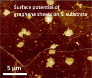
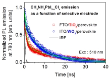
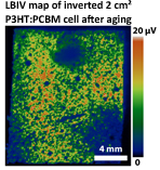
In addition to conventional technologies used for the physical chracterization of components, the ELITE team focuses on several original tools for the advanced understanding of the underlaying physical mechanisms. The group exploits for example an atomic force microscope (AFM) which can be used in a high-resolution Kelvin probe mde (HD-KPFM). This equipment is particularly suited for the estimation of electrode work functions or surface potentials of hybrid composite layers (see the left-hand side image below). In parallel, the group is interested on charge kinetics associated with various assemblies, by characterizing model devices using time-resolved techniques (see the PLATINOM technological plateform) such as time-resolved photoluminescence or transient photo-voltage / photo-current measurements. One objective is to evaluate the lifetime of photoexcited species, as well as their interactions with their environment in presence of a specific interface (see central image below). Finally, the group also exploit LBIC/LBIV mapping (light beam induced current and voltage), which allows to image the electrical response of a solar cell at the module level. THis technique is highly relevant to reveal specific fabrication faults or the degradation behaviour of devices (see right-hand side image below).
Material and device modeling
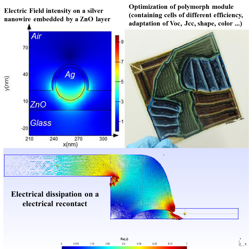
The numerical simulation of physical processes allow us to define new optimization strategies for our optoelectronic devices. Conventional electromagnetic models can thus be taken into account for any structure and for any applied field, via a "transfer-matrix" methodology for calculations or using Finite-difference Time-domain methods (FDTD, see images below). Specific dissipative physical models, coupled to active models for the implementation of photon/electron conversion processes, are applied in order to evaluate the impact of the device design, layer thicknesses, and nature of materials on the performance of final devices (solar cells, light-emitting diodes, etc).
Collaborations and partnerships
Local collaborations
Teams @ XLIM: MINT (Axe RF-ELITE), ReSYST team (Axe Systèmes et réseaux intelligents) ; Equipe GPPMM (Photonique) ; Equipe Photonique-Fibre (Photonique) ; LabEx SigmaLim ; Laboratoire SPCTS (oxydes de pérovskites, micro-sources, etc) ; Laboratoire LCSN (matériaux pi-conjugués) ; INSERM UMR 850 ;
National and international collaborations
IMS (Bordeaux) ; CEA (IRAMIS/NIMBE de Saclay, SYMMES de Grenoble) ; PCM2E/Université de Tours ; LAC - PPSM / ENS Cachan ; IKAMBA Organics ; SOLARONIX ; IMMM/Université du Maine ; IM2NP (Marseille) ; CEISAM (Nantes) ; CINAM (Marseille) ; FOTON (Rennes) ; EDF ; DISASOLAR ; CERADROP ; ICGM Montpellier ; Université de Mons ;
Queen's University ; University of South Africa (UNISA) ; Jan Dugloz University (Pologne) ; Imperial College London (UK) ; Kanazawa University (Japan) ; Université de Constantine 1 (Algérie) ; Université de Sétif (Algérie); Université de Tizi Ouzou (Algérie) ; Université de Rabat (Maroc)
![]()


![]()
 UMR CNRS n°7252
123, avenue Albert Thomas - 87060 LIMOGES CEDEX.
Tél. +33(0) 587 50 67 00 - Fax +33(0) 555 45 76 97