MINACOM Department
You are here
Plastic Optoelectronics
The “Plastic Optoelectronics” project carries out experimental and fundamental research on organic electronics, from device implementation, and optoelectronic characterization, to the modeling of the involved physical properties. Specific technologies are developed in order to implement the main organic optoelectronic devices:
- Organic Light-Emitting Diodes (OLEDs) for flat panel display and low-consumption lightning applications
- Organic Field-Effect Transistors (OFETs) to be used in logical circuits or RFID memories
- Organic and Hybrid Solar Cells (OPV) for renewable energy production in nomad applications or unconnected grid components. See the demonstration video...
Our activities are mainly developed within local, national and international collaborations with academic, as well as industrial partners.
Group members - Seminars - Internal web pages of the group - Intranet Platinom
Specific technologies
Ion Beam Assisted Vapor Phase Deposition (IBAD)
Contact: Rémi Antony
Most of the optoelectronic devices use vacuum-deposited metallic cathodes (Ag, Al, etc.). Ion beam assisted vapor phase deposition (IBAD) aims at simultaneously deposit a metal by evaporation on a substrate while submitting the substrate to a beam of energetic ions (Ar+, N+, etc.). Using this technique, the optical, electrical, mechanical and chemical properties of the deposited layer are modified. In particular, IBAD allows a densification of the deposited cathodes resulting in lower oxygen and moisture diffusion within the active layer, hence improved lifetime.
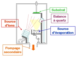
Principle of IBAD
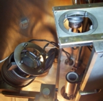
Transparent conducting electrodes deposited by IBS
Contact: Bruno Lucas
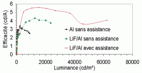
Important efforts are today devoted to the fabrication of transparent conducting oxides (TCO) and multilayered electrodes (ITO/Ag/ITO or ITO/Au/ITO). In this context, deposition methods based on ion beam sputtering (IBS) have been developed in the group. These techniques allow the achievement of TCO at low temperatures presenting a good transparency and significant conductivity required in OLEDs or OPV. A control of the electrode properties using IBS at low temperatures is crucial in order to improve device performance and to allow the commercial emergence of plastic optoelectronics. Flexible light emitting diodes (OLEDs) based on IBS-deposited electrodes and presenting a luminance of more than 20 000 cd/m² have been obtained in the group (400 cd/m² for a typical display).
IBS experimental set-up
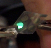
Flexible OLED based on IBS-deposited ITO
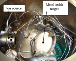
Fabrication of semi-conducting inorganic nanostructures from solution
Contact: Johann Bouclé
Hybrid devices, which exploit physical properties of both organic and inorganic materials in a single device, demonstrated a strong potential for applications in optoelectronics. In this context, we are interested in the synthesis from solution (sol-gel) of metal oxide nanocrystals presenting well-defined morphologies to be used in the active layers of our devices, as well as by the deposition by spray pyrolysis of inorganic thin films that can be implemented as transparent conducting electrodes, or blocking/buffer layers in our photovoltaic cells, organic transistors or light-emitting diodes.

Solution-processed ZnO nanocrystals
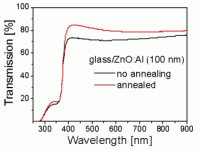
Optical transmission of Al-doped ZnO thin films
New technologies under development
- Pulsed Laser Deposition (PLD) of organic Materials (contact: Catherine Di Bin)
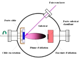
Principle of PLD
Pulsed laser deposition (PLD) is a versatile technique that can be used for the deposition of thin organic layers: it takes advantage of the possibility to control the layer thickness and to obtain films with good crystalline and optical quality at room temperature. In order to avoid the degradation of the organic layer, it is necessary to use low laser fluence, close to the fluence threshold (a few mJ/cm²). Pulsed laser deposition can also allow selective etching of already deposited organic layers by using suitable shadow masks.
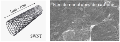
- Fabrication of transparent conducting electrodes based on carbon nanotubes (contact: Rémi Antony, Bernard Ratier)
Regarding their electrical properties, single-walled carbon nanotubes (SWCNT) can be either metallic or semiconducting depending on their geometry (diameter and rolling arrangement). The use of such carbon nanotubes deposited as thin layer on glass substrates to replace conventional flexible transparent conducting electrodes was shown to be a fruitful strategy, especially for OLEDs. In this context, we now develop CNT-based electrodes from solution in the group, in order to demonstrate alternative transparent electrodes at low cost.
- Fabrication of organic-inorganic hybrid composites using physical methods (contact: Bruno Lucas, Johann Bouclé )
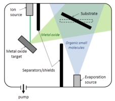
Principle of the co-deposition technique
New strategies of hybrid components have been developed to address the intrinsic limitations of organic materials (lifetime, stability, etc.). In the group, we propose a new approach to hybrid devices by co-depositing an organic material by vacuum evaporation and an inorganic compound by ion beam sputtering (ZnO, TiO2, etc.). Such hybrid layers can also act as encapsulation barriers of plastic devices.
Organic Optoelectronic Devices
Organic and Hybrid Solar Cells (OPV)
Contact: Bernard Ratier, Johann Bouclé
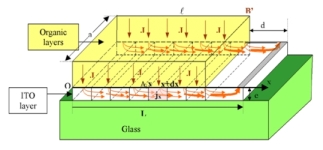
Photovoltaic cells convert incident light energy into electrical energy through photon absorption, free charge generation and finally charge transport in an active layer based on the association of an electron donor and an electron acceptor material. Organic solar cells, based on small conjugated molecules or semi-conducting polymers, take advantage of low-cost processing routes and can be deposited on flexible substrates. The ?Plastic Optoelectronic? project is actively involved in the development of organic and hybrid solar cells through various national financial programs ADEME-CEA, ANR and DGA, and is part of the ?NANORGASOL? CNRS network. Device fabrication, as well as photo-physic characterizations, are realized on site under inert atmosphere (glove box): physical deposition by co-evaporation, spin-coating, I(V) characteristics under simulated standard solar emission, external quantum efficiency measurement, transient photo-voltage and photo-current, etc.
Concerning organic solar cells, our main objectives are:
- The control of the active layer morphology at the nanoscale, for devices based on both small evaporated molecules (CuPc:C60) and on conjugated polymers (P3HT, MEH-PPV, etc.) with soluble fullerenes (PCBM)
- The electrode optimization using ion beam based techniques (Ion Beam Sputtering IBS, Ion Beam Assisted Deposition IBAD)
- The modeling of the active area in order to improve their performance and lifetime
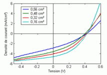
Our current work focus on the development of polymer/carbon nanotubes composites and on the optimization of polymer/fullerene bulk heterojunctions (P3HT:PCBM) which allowed us to demonstrate power conversion efficiencies up to 5%.

I(V) characteristics of a P3HT:PCBM bulk-heterojunction
Optimization of electrode design on small molecule-based solar cells
IIn parallel to organic devices, we also initiated the development and physical characterization of hybrid solar cells based on nanostructured metal oxides (TiO2, ZnO, etc.). We mainly explore solid-state dye-sensitized solar cells (SSDSSC) which present a strong potential as competitive alternatives to inorganic or all-organic photovoltaic devices. In parallel, we also develop conventional hybrid devices, such as polymer/nanocrystal blends. Our main efforts aim at better controlling the interfaces (SAMs, dipoles, etc.) at the nanoscale by developing organized nanoporous metal oxide architectures from low-cost deposition methods (sol-gel, spin-coating, doctor-blading, etc.).
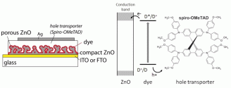
Structure and simplified energy level diagram of a ZnO-based solid-state dye-sensitized solar cell
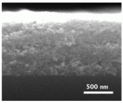
ZnO porous layer deposited from solution
Organic Field-Effect Transistors (OFETs)
Contact: Thierry Trigaud, Bruno Lucas
We develop new technologies for the fabrication of optoelectronic circuits based on organic thin film filed-effect transistors (OFET). Our main goal is to achieve alternative solutions processed at low cost due to inexpensive starting materials (organic materials) and processing routes.
From the experimental point of view, two main topics are developed in the group:
- Transparent organic filed-effect transistors
- Flexible circuits obtained through printing techniques (serigraphy
From the theoretical point of view, we are interested in:
- The physics of organic semi-conductors (charge transport, mobilities)
- The printing techniques and their accuracy (40 µm using serigraphy)
- The interface states which depend on the deposition technique used and on the materials
- The architecture of organic logical circuits
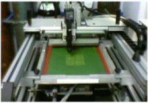
Deposition bench by serigraphy of organic transistors (compatible large area)
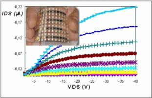
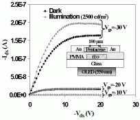
Typical output characteristics of a flexible organic OFET
IIn parallel, we also develop advanced components based on organic transistors, such as photo-transistors. Various effects can indeed result in the bulk from photon absorption or emission, such as photo-conductivity or photovoltaic effect, which directly relate to transport mechanisms. In this context, the photo-transistor exploits the photo-conductive properties of the transistor active layer. This component, possibly flexible, can be used as light-controlled switch, optical grid amplifier, detection circuit or sensor.
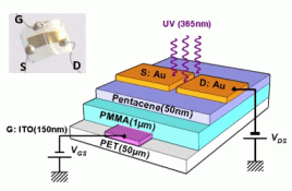
Flexible organic photo-transistor under light excitation
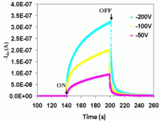
Transient response of the photo-transistor various drain voltages as a function of illumination
Organic Light-Emitting Diodes (OLEDs)
Contact: Rémi Antony, Bruno Lucas
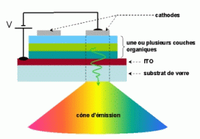
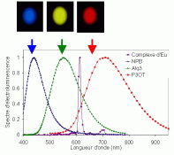
Organic light emitting diodes (OLEDs) convert electrical energy into light. The typical active layers are composed by one or several organic films sandwiched between a metallic and a transparent electrode. Applying an electric field to the electrode allows the injection of charge carriers which will recombine to form an exciton. This quasi-particle can generaly desexcite radiatively in 25% of the cases. The wavelength of the emitted light, as well as the optoelectronic parameters, depends on the active layer properties. OLEDs based on small molecules, rare earth complexes, or semi-conducting polymers take advantage of low-cost processing routes, and of the possibility to use flexible substrates.
Electrical characteristics of a photo-coupler in the dark and under illumiation
We also develop OLED-based optoelectronic devices presenting advanced functions. Photo-couplers, which are obtained by coupling two organic components deposited on the same transparent substrate, are a perfect example: a light-emitting diode (OLED) is used as input unit and a thin film transistor (OTFT) as output unit. These devices can be used to transfer information in a system without electrical contact. Moreover, the development of these new organic devices allows assessing their performance in terms of lifetime and thermal stability.
Advanced characterization techniques
Charge mobilities, transport mechanisms
Contact: Bruno Lucas
Performance of o ganic devices depends on different parameters, which occur at different scales. At the supra-molecular scale, the charge mobility drives recombination processes in OLEDs and charge collection in photovoltaic cells. Thus, organic device performance is strongly sensitive to charge carrier mobility. In order to extract this parameter, we develop a new method based on dielectric measurements: the extrapolation at low frequency of the dielectric losses allow the estimation of the static conductivity.Then, the charge carrier density is extracted from the I(V) characteristics, in order to finally evaluate the charge mobility.
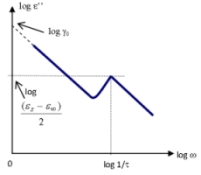
Dielectric losses versus frequency

Experimental I(V) curve of a ITO/Alq3/Al structure
Transient photo-voltage/photo-current measurements
Contact: Johann Bouclé , Catherine Di Bin
In an attempt to better understand and control the physical processes which govern organic and hybrid solar cell performance, we developed in the group transient photovoltage and photocurrent measurements. From this advanced characterization technique, we can extract the relevant parameters that describe charge recombination at the donor-acceptor interface (charge carrier lifetime, recombination rates, etc.), as well as charge transport processes (transit time, estimation of charge carrier mobilities, etc.) within the active layer of working devices. These studies aim at better relate the experimental parameters of photovoltaic devices, either organic or hybrid, to the key mechanisms driving their intrinsic performance.
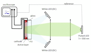
Principle of the transient photovoltage measurement
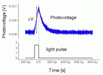
Typical photovoltage transient of a P3HT-ZnO hybrid solar cell
Characterization and optimization of device lifetimes
Contact: Bernard Ratier, Rémi Antony
The stability of organic optoelectronic devices remains a major technological limitation to overcome in order to develop realistic commercial applications. Several strategies are employed, such as the development of flexible substrates and hyper-barrier encapsulation systems. In the group, we mainly focus on strategies that aim an improvement in the intrinsic device lifetime, by using design optimization procedures and advanced fabrication techniques: use of buffer layers at the interfaces, densification of active and electrode layer using ion beam assisted techniques, etc.
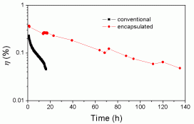
Optimization of an organic solar cell lifetime through improved electrode design
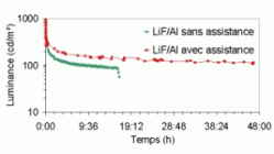
Time evolution of an OLED with and without ion beam assisted cathode
Modeling
Physical modeling of optoelectronic devices
Contact: Bernard Ratier
The numerical simulation of the different physical phenomena involved by the optoelectronic processes that occur in the devices can potentially allow the emergence of new strategies towards the optimization of organic components. In this context, the main approaches we are currently developing are:
- The modeling of the optical field in photovoltaic cell active layers (collaboration TECSEN, UMR-CNRS 6122, Université Paul Cézanne Aix-Marseille 3)
- The modeling of the electromagnetic field both in the device and in the electrodes, as well as in new cell geometries (collaboration PPF Cellules solaires photovoltaïques plastiques, Laboratoire POMA, UMR-CNRS 6136, Université d?Angers, collaboration avec le projet MACAO du département XLIM-MINACOM)
Moreover, numerical simulations of growth mechanisms that occur during organic layer deposition are a powerful tool for the improvement and optimization of the deposition conditions.
Modeling of current density lines in the anode of an organic solar cell

Current mapping obtained by numerical simulation
![]()


![]()
 UMR CNRS n°7252
123, avenue Albert Thomas - 87060 LIMOGES CEDEX.
Tél. +33(0) 587 50 67 00 - Fax +33(0) 555 45 76 97